
Reversing a Printed Circuit Board is not that easy and is indeed tough for beginners. One needs to have an in-depth knowledge of the software of the circuit design to carry out the process efficiently. Having a detailed idea about the different hardware backgrounds of the circuits is equally important. There will be a lot of issues during the reverse engineering process,and for that, you need to know how to deal with them. In this post, you will get to know about the steps that engineers will need to follow for the reverse engineering process.
Start Clicking Pictures (Higher Resolution Is Better)
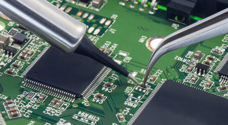
First things first, you need to take bright pictures of both sides of the Printed Circuit Board (PCB). Make sure you get a high-quality picture output, which is less blurry or noisy. If you are thinking about using a scanner, well do not expect to get the best results. Most of the time, the surface of the PCB is undulated and therefore scanning it will not give good results.
Start Editing Your Pictures With An Editing Tool
After you complete taking pictures, you need to load them into your chosen editing tool. After importing the picture, firstly, you need to crop the edges out so that you get the perfect material only. Zoom in further cut the minute edges too, and reduce the level of transparency as needed. At the end of it all, you will have for you the PCB shot that you need.
Start Blending The Pictures
Depending on which editing application software you are using, you should choose the option that will blend the images. Now, there is not much to tell in this part as this differs from app to app. However, if we consider the Screen Blend option of the Adobe Fireworks app, then you need to down the contrast to 50{061df1cae2d64927061e07b6d7eafcef06a76bc18c3ebe725bd65677dd35588a}. Start to highlight the traces of Copper and then blend,as said.
Start Brushing The Network Of Lines
So, now that you have highlighted the traces of Copper, all you need to do is use the Brush tool. The Brush will help in making the network of lines visible. After you get to see the intensity, you are good to run the software on the circuit.
This process is tougher than it appears theoretically, so you better hire experts from the likes of Fast PCB Studio. Their professionals will undoubtedly do it better, have trust in that.